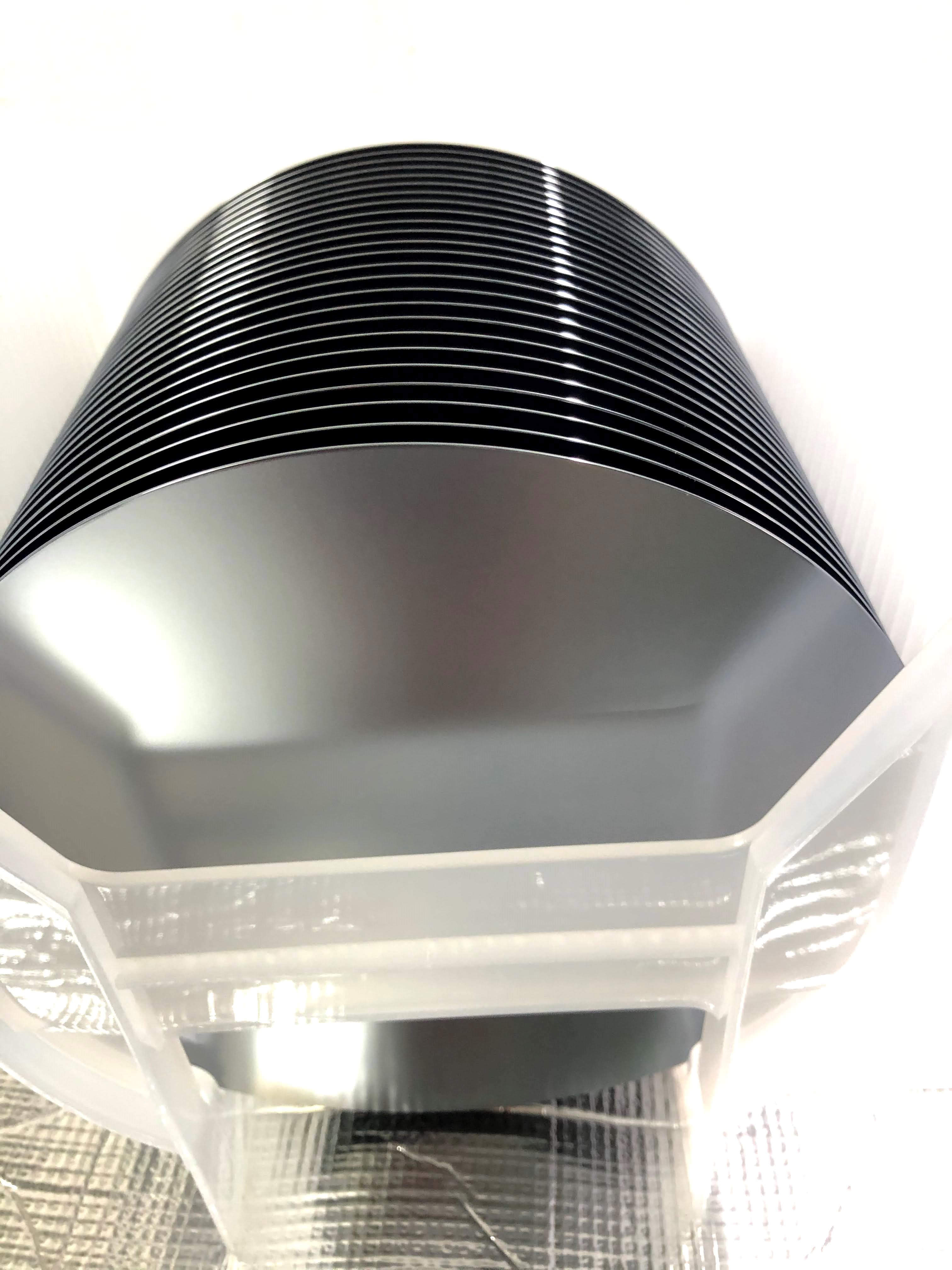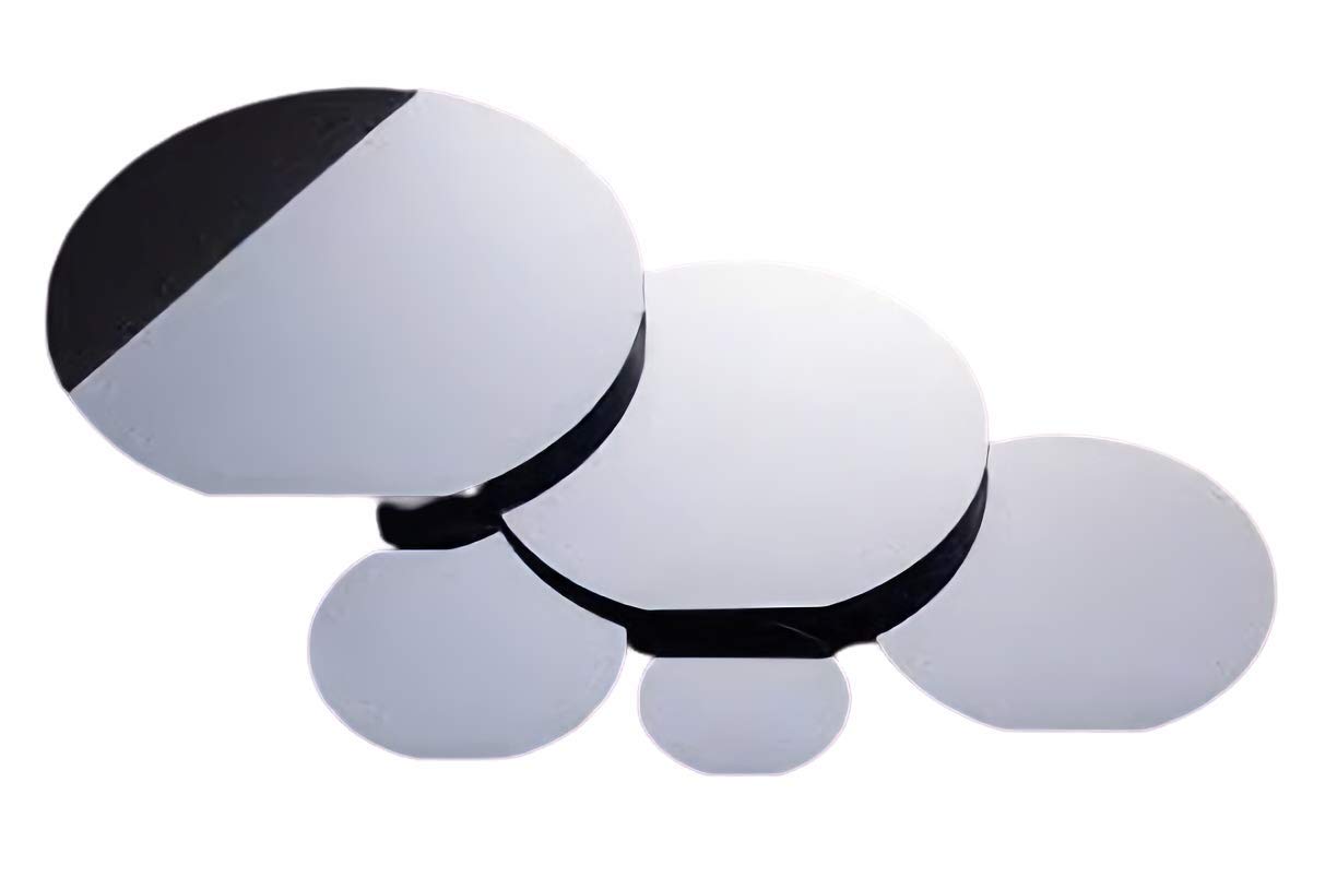
Silicon wafer
We handle various wafers made by Japanese manufacturers with a diameter of 100 mm to 300 mm.
The
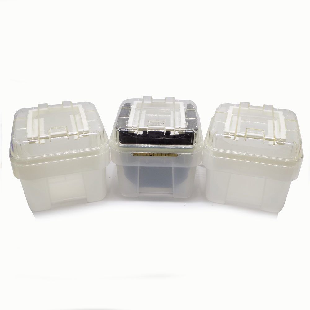
following are just examples, such as in cassettes (lamy packs), dummies, and for testing (in styrofoam containers) . Please contact us for your desired product according to your application.
Product Specifications
| item | Unit | specification | ||||
| size | inch inch | Four | Five | 6 | 8 | 12 |
| Manufacturing method | – – | CZ / FZ | ||||
| type | – – | P or N | ||||
| Dopant | – – | B / P / As / Sb / Non-dope | ||||
| Crystal orientation | – – | 100/111/110 / | ||||
| Thickness | μm | 525 | 525/625 | 625 | 725 | 775 |
| Thickness tolerance | μm | twenty five | twenty five | twenty five | twenty five | twenty five |
| Resistance values | Ω ・ cm | 0.001-10000Ω | ||||
| Orifura | – – | ○ | ○ | SEMI or Jeida | notch | notch |
| particle | Lv | 0.2um @ 50ea, 0.09um @ 50ea | ||||
| Surface condition | – – | Single-sided mirror / Double-sided mirror | Double-sided mirror | |||
| quantity | lot | 25 sheets / case | ||||
| type of packing | – – | Wafer case + clean pack | ||||
| remarks | – – | * Please contact us for high precision wafers. | ||||
| * Please contact us for low particle wafers and film attachment. | ||||||
| stock | – – | ○ | ○ | ○ | ○ | ○ |